

THE PROCESS
HARDWARE AND TOOLS USED
- Autodesk EAGLE 8.6.3
- Adobe illustrator
- Fab module
- Universal gcode sender
- DIY CNC GRBL cnc that use GRBL CNC Shield.
1 x FR1 (Copper PCB Board).
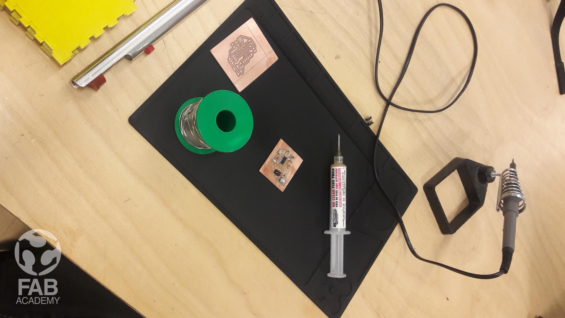
- Soldering kit ( Soldering iron,soldering wire, Solder Wick, Soldering flux, Soldering Iron stand,Vise,Solder Sucker,Tweezers )
- 1 x 1/64 inch end mill bit (Titanium Coated Carbide PCB Engraving CNC Bit by 1/64 Inch Autek 10x Router Tool 30 Degree 0.1mm Tip(J3.3001Tix10) by Autek )
- Double-Sided Tape.
- AVO multimeter.
REDRAWING THE ECHO HELLO-WORLD BOARD
SCHEMATIC DESIGN
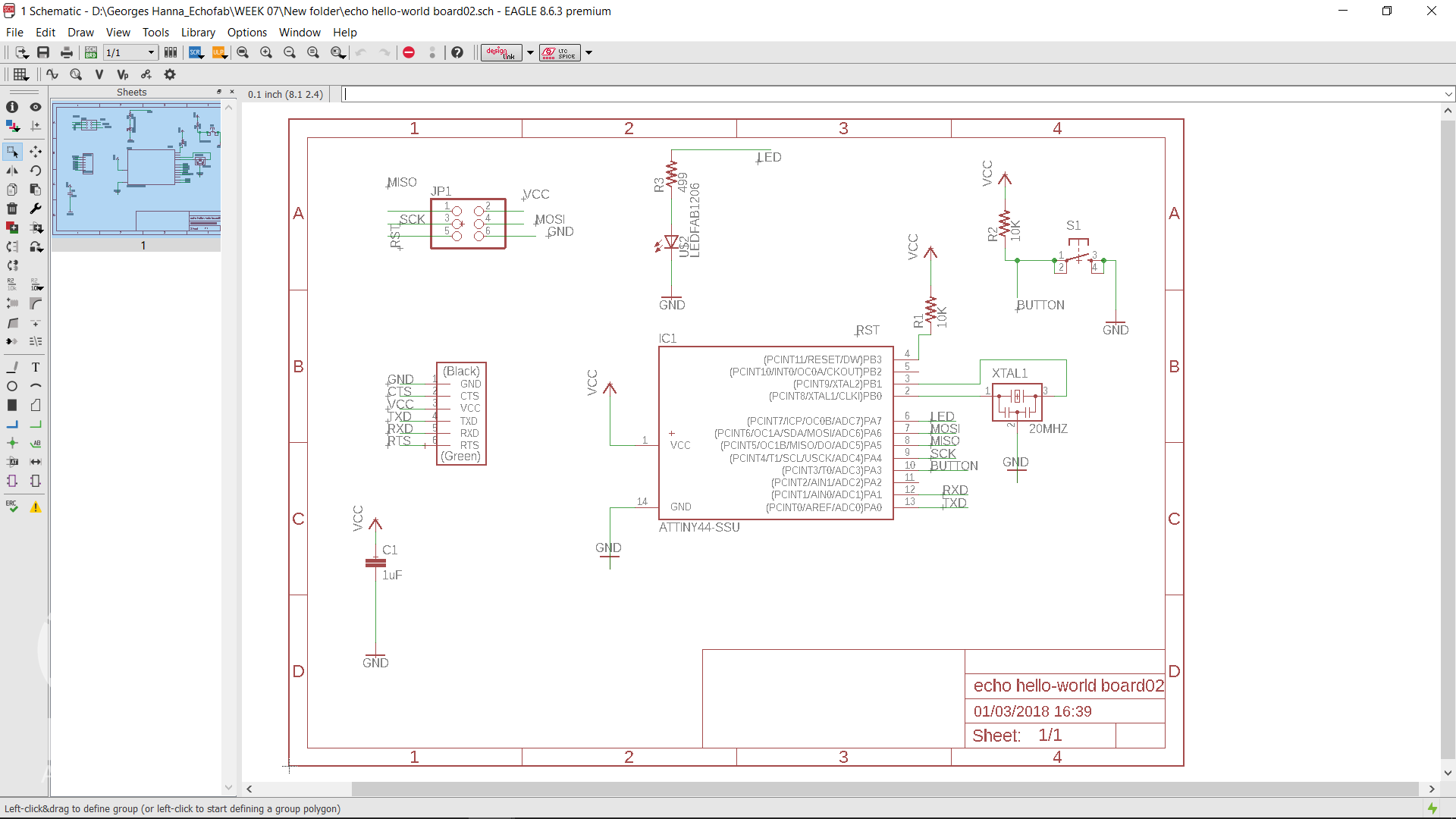
Our task for this week was to design hello-world board in addition to that we were asked to add one LED and one button into our design. To start with designing the board first I had to choose the electronic design software, I decided to choose eagle since it is user friendly and it has a plenty of free tutorials online.
To begin with, First I had downloaded Eagle software and I followed the tutorial that was provided by our mentor at echoFab you can find the link for this tutorial by clicking HERE.
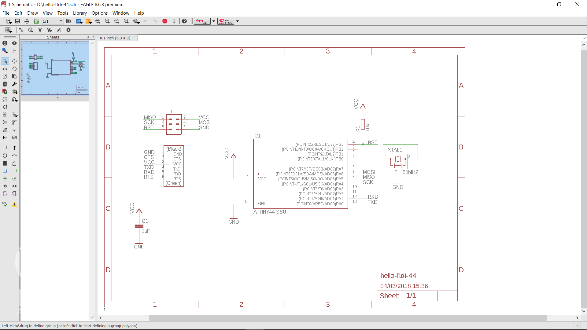
As the tutorial suggests, I downloaded the example file that called ( Hello Echo example ) so we can build on that file. (image # 01)
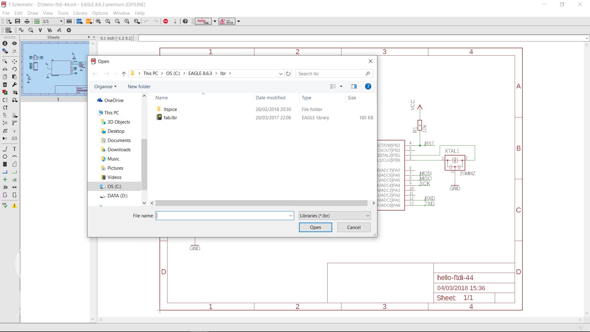
Then I had to download and install the component libraries the download link for downloading the library is mentioned in the useful tips and links section. The challenging part was knowing which component I have to use because later on each component will represent the physical dimensions of our board layout. This is the area where we’ll place all of our components together this is why it is very important to use the right components so they can match the exact dimensions of the real ones when milling the board. You can find more information about the settings and tools I used in eagle by going to to my input devices week page.
Below are all the components that I had used :
- ATtiny44-SSU
- 20mhz resonator: ATtiny has an inbuilt 8mhz clock, but this one is faster and more accurate
- 6mm Switch Omrom
- AVR ISP SMD header: for programming the board
- FTDI SMD header: powers the board and allows it to speak to the computer
- 10K resistor x 2
- 1µF capacitor
- 499 ohm resistor
- Blue SMD led
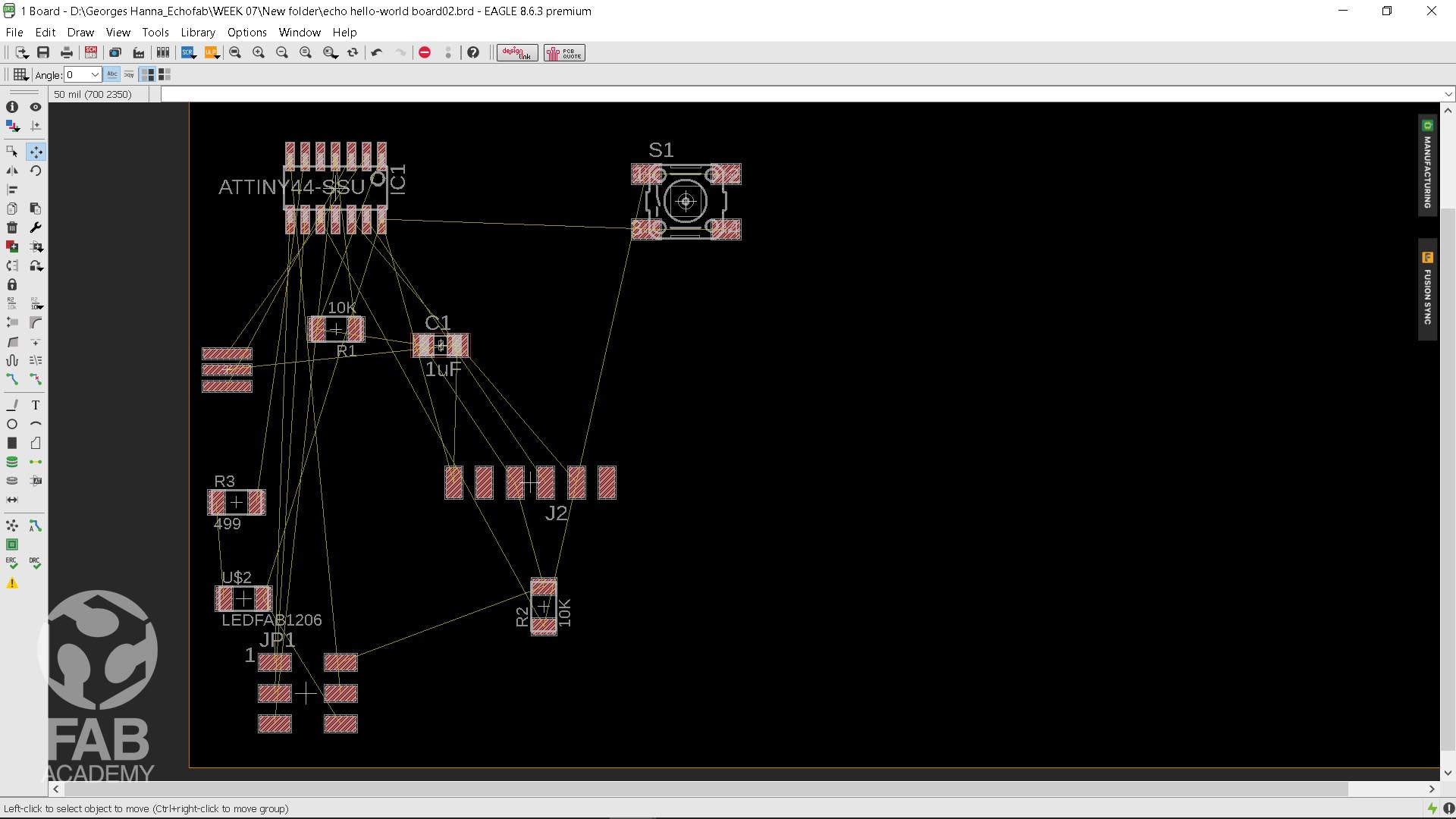
BOARD DESIGN
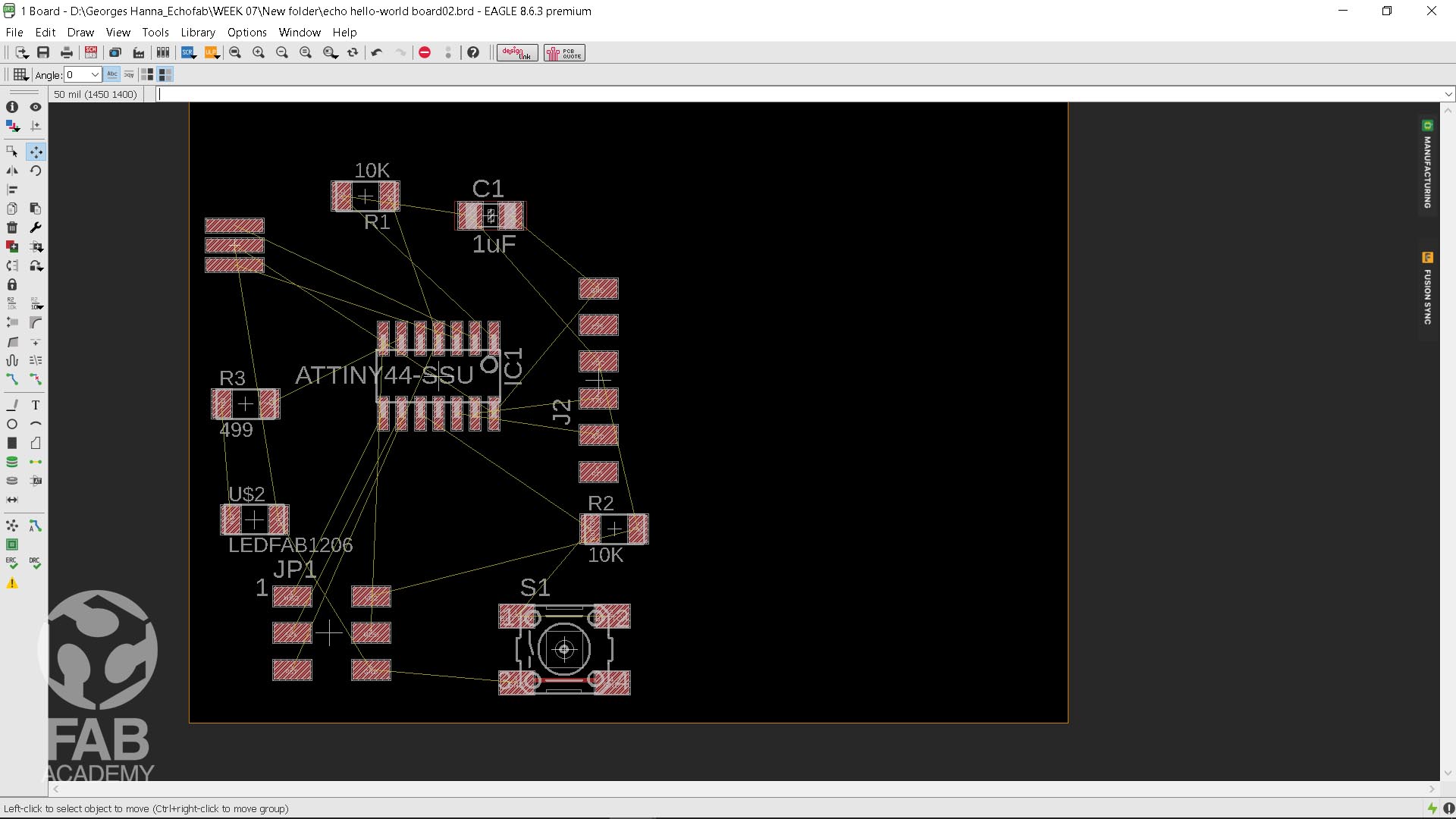
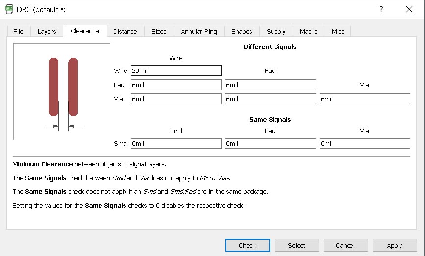
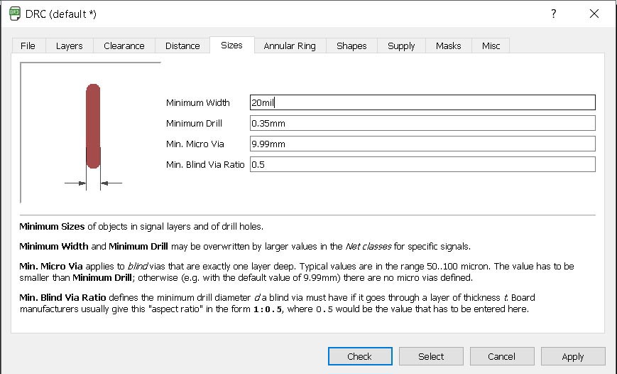
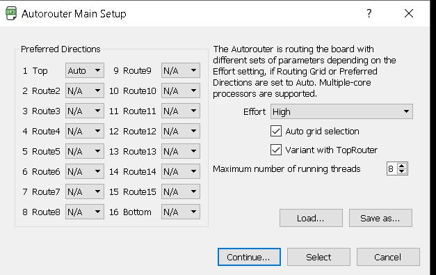
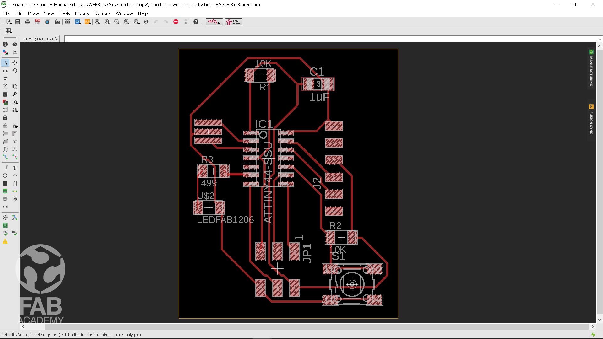
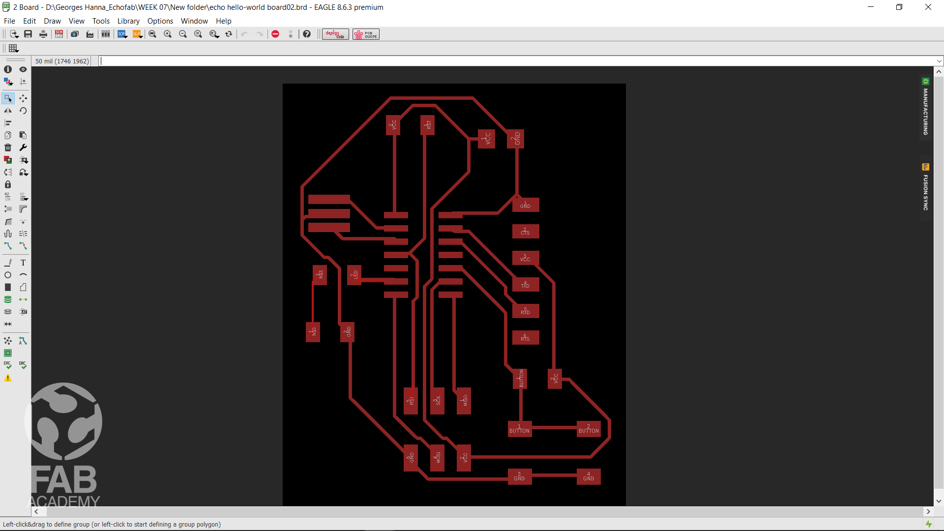
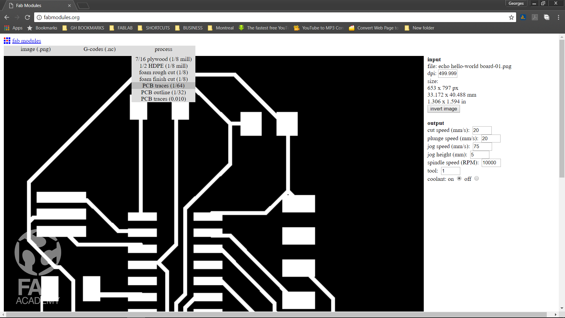
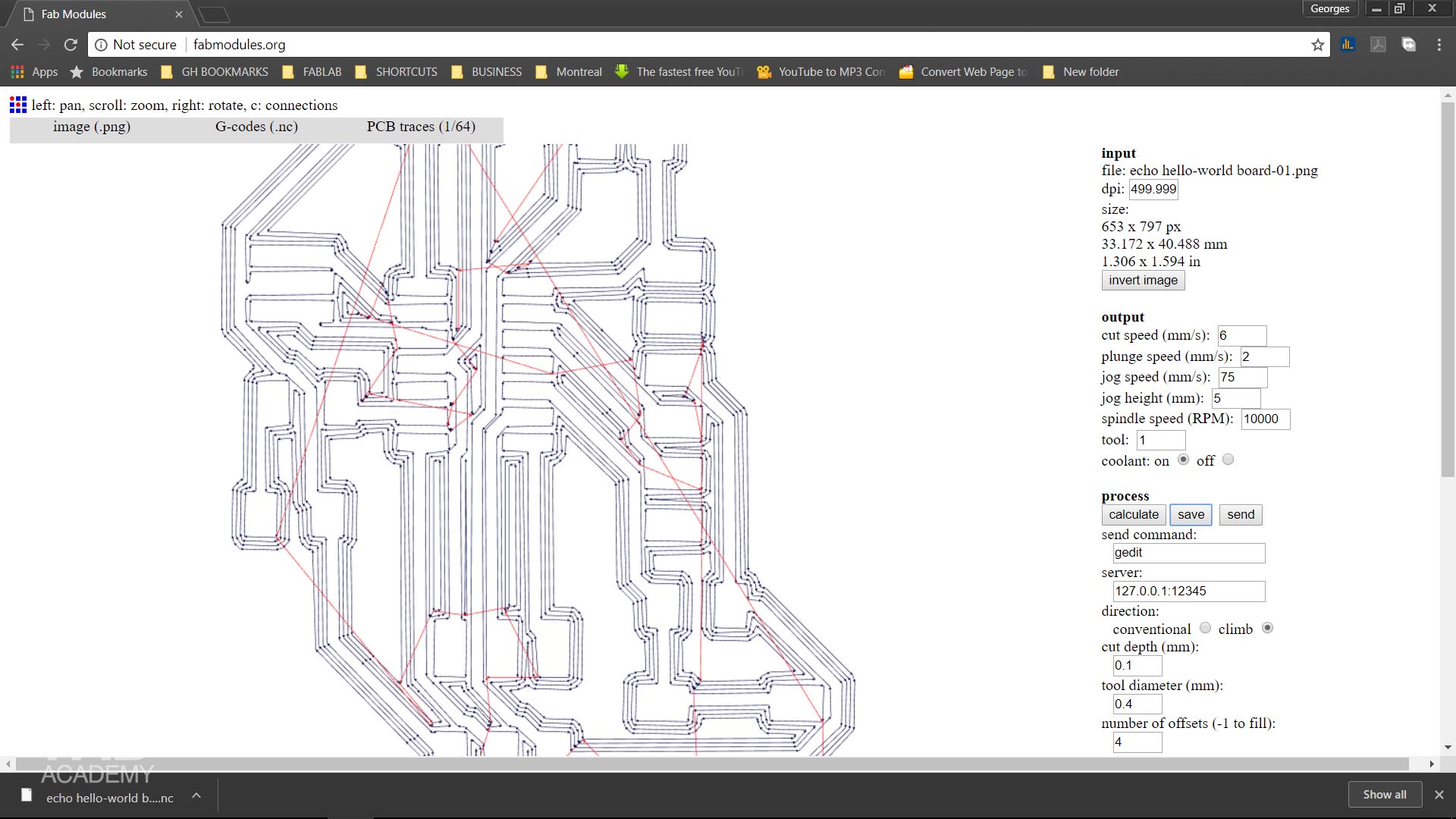
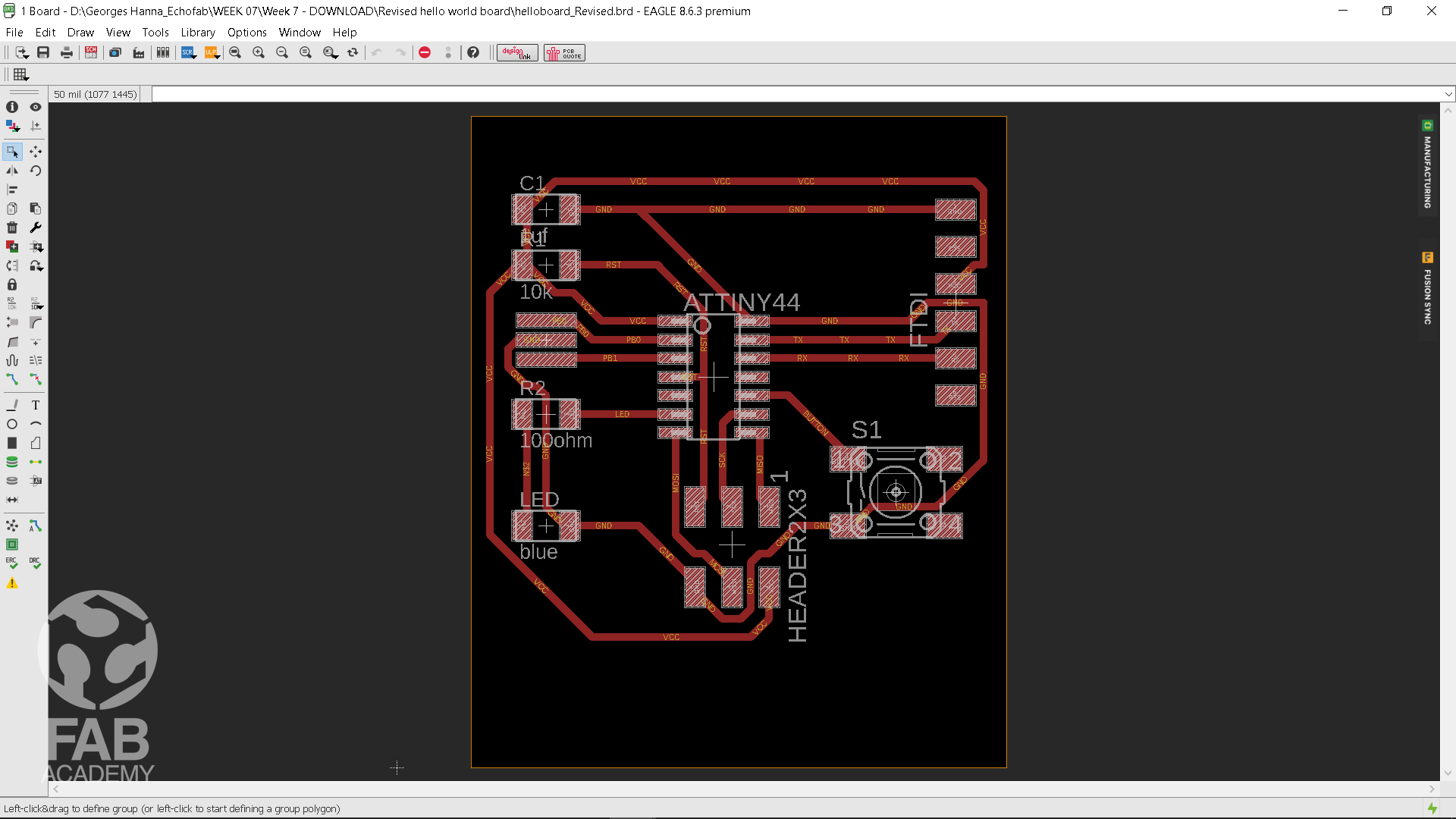
After finalizing the schematic design and connecting all the parts together I had switched to the board interface from the schematic. You can do that by simply using the command line typing board or using the menu pressing Generate/Switch to board. Since I'm novice at electronic design I decided to use autoroute option. To start with first I had to adjust DRC ( Design rules ) because they define all the parameters that the board layout has to follow. And they allow us to adjust some vital values like clearance, distance, sizes and shapes Images # 06 & Image # 07 show the DRC settings I used before using autorouting tool (image # 08 ). Then when I was done with adjusting my settings I thought that routing the lines between all components is an easy task in a matter of a few clicks I'll get the board ready but I was wrong. Routing was a really a tough process I spent a couple of hours trying to find the ideal position of the components but failed to success . To solve this issue and after reading many tutorials I decided to keep connections as short as possible and I started to use Ratsnest tool every time I adjust the placement of the parts and once I used autorouting again everything seems to work super fine it was able to route everything without producing overlaps. Finally, After finalising the board design I turned off all the unnecessary layers as seen in image # 10 and I exported the traces in 500 DPI resolution PNG format in order to open it in Fab Modules.
MILLING THE PCB
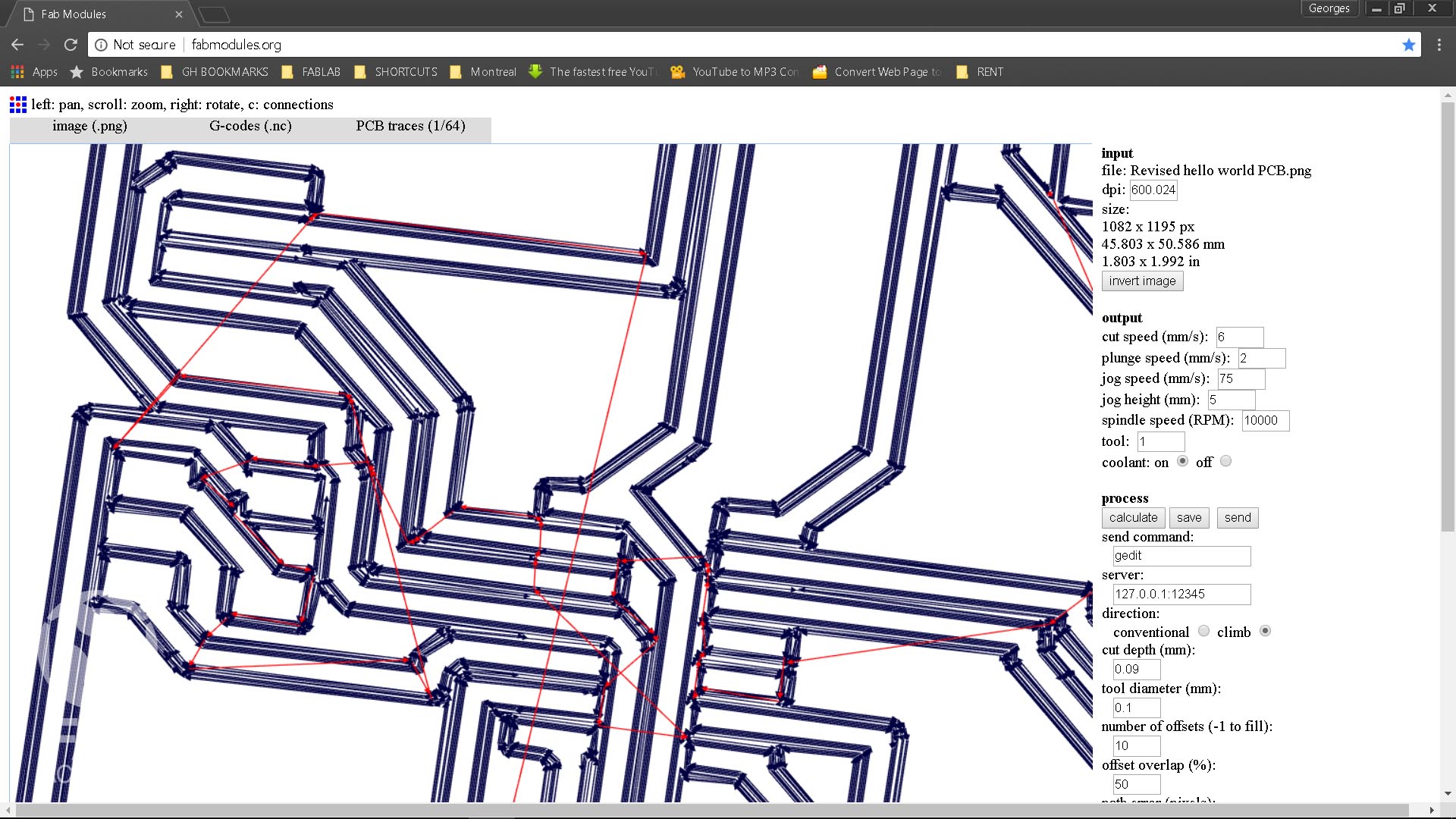
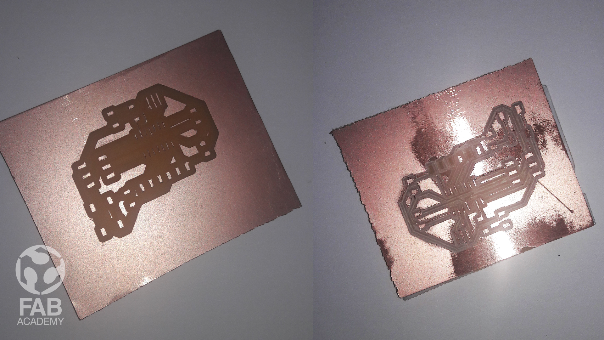
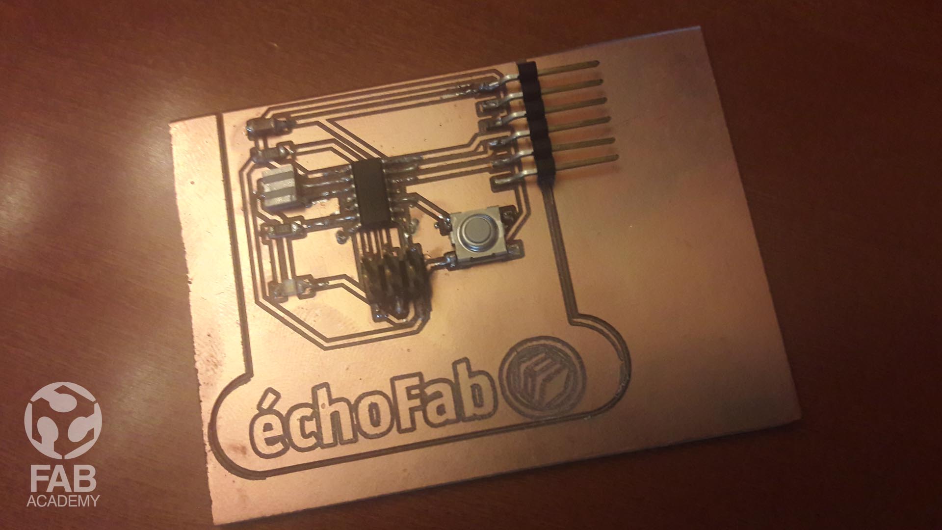
Milling the PCB using our DIY CNC was so tricky and not fun at all because of many factors like we had to zero the machine out manually since the machine doesn't have a touch plate in addition to that the machine’s table was not leveled out correctly so we had really difficult times configuring and adjusting the machine. Even though, We were using brand new bits but still in he first weeks we couldn't get what we were looking for. For instance, sometimes when we were zeroing the 3 axis out and telling the machine to move back to point 0 it was moving in a wrong direction because of that we had to shut down the connection quickly from FAB MODUAL console in order to stop it immediately since it has no emergency button as a result we were a way behind with our PCB production projects and they were postponed . After spending a few weeks trying to understand how it interprets the code we send ( G-code) we decided to tweak the settings in Fab Modules and to try with different settings. So after many trail and error we found the ideal settings which let us achieve convenient results. Below is a list of the ideal setting we used with our machine : CUT SPEED (mm) : 6 CUT DEPTH (mm) : 0.1 TOOL DIAMETER (mm) : 0.4 NUMBER OF OFFSETS : 4 Recently, Few weeks before the ending of Fab Academy classes our instructor Mathieu milled a new wooden table for the CNC as a result we started to have a much better and promising milling quality as seen in image #20 This revised board was milled and programed after me and my friends ( Marc Lemair and Geoffroi Garon-Épaule ) were facing difficulties programming our first hello world board. NOTE : For the revised Hello world board we followed exactly the same steps as in the initial board. Overall, It was a good learning experience and now I'm really satisfied with the end result.
SOLDERING THE COMPONENTS
For soldering the parts, I followed the strategy I followed in the electronic production week
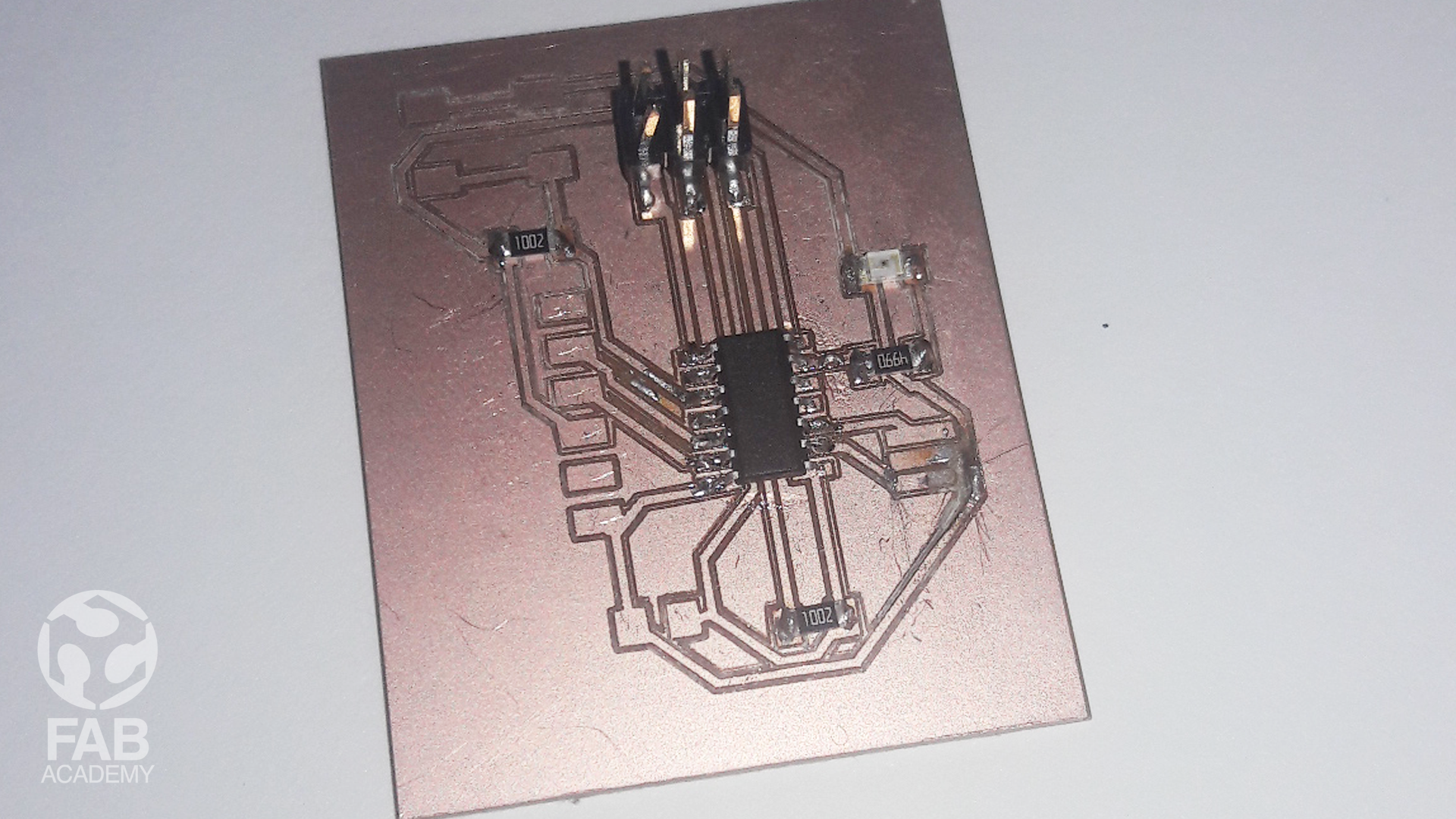
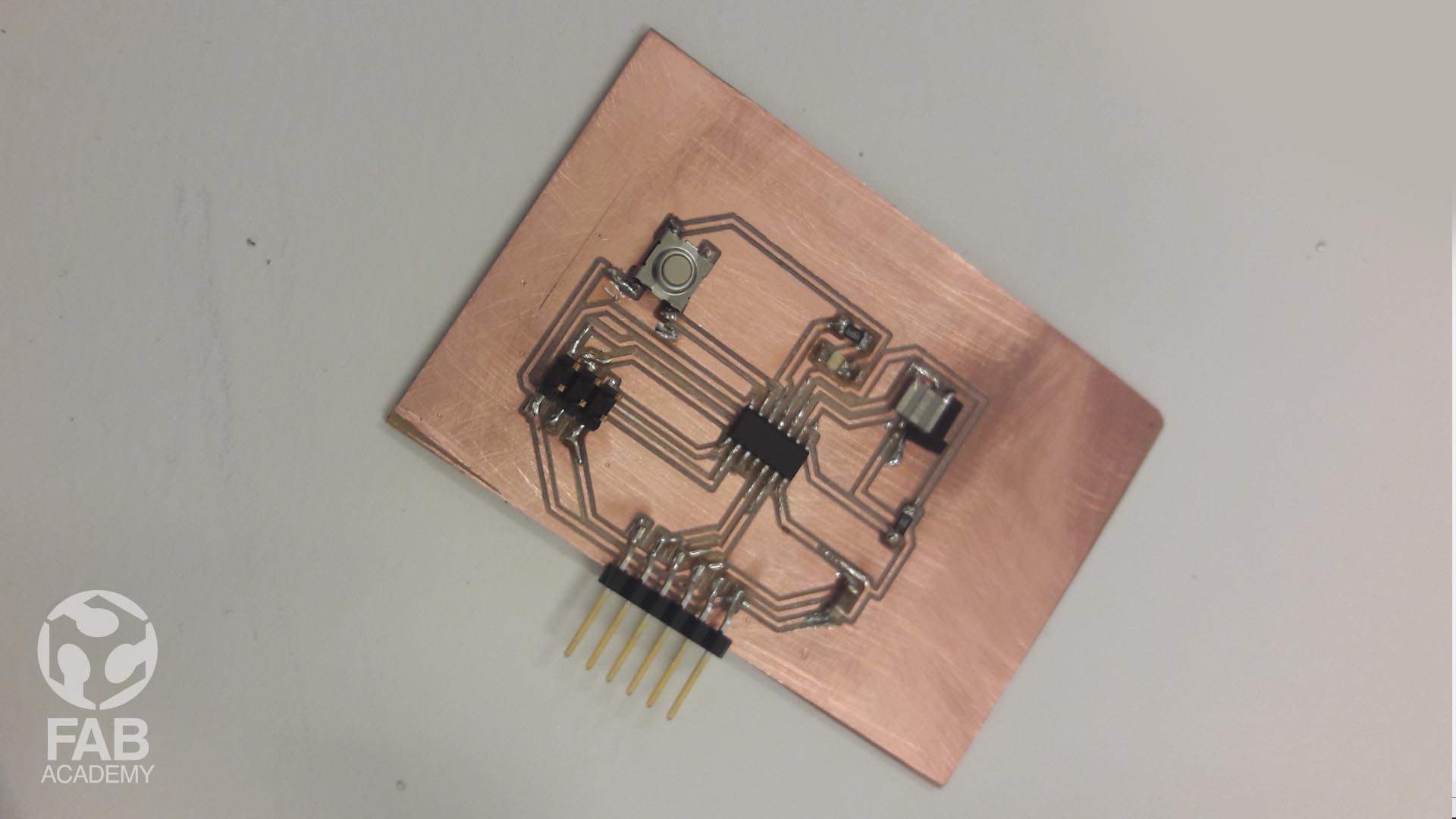
First, I collected all the needed components and I started with the most difficult parts to solder and when I was done with the big parts I started soldering from the smallest to the bigger parts :
1 - 1 x Attiny 44
2 - 1 x 470Ω SMD Resistor
3- 1 x 10mF SMD Capacitor
4- 2 x 10kΩ SMD Resistor
5- 1 x blue SMD LED
6- 2 x 3 SMD Pinheader
7- 1 x 6 THT Pinheader
8- 1 x SMD button
9- 1 x 20mhz resonator
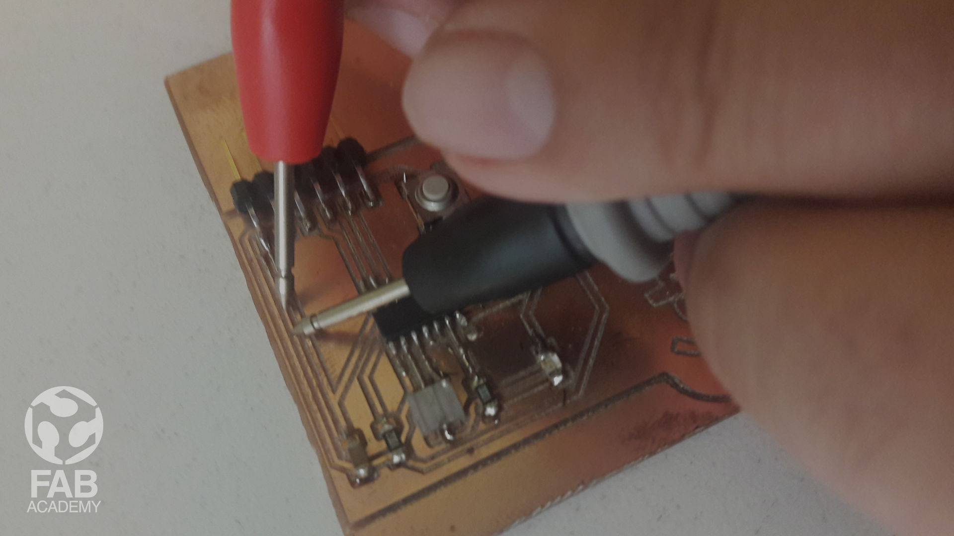
During soldering I was using a multimeter regularly to assure that I don’t have any short on my circuit board .
TESTING THE CONNECTIONS
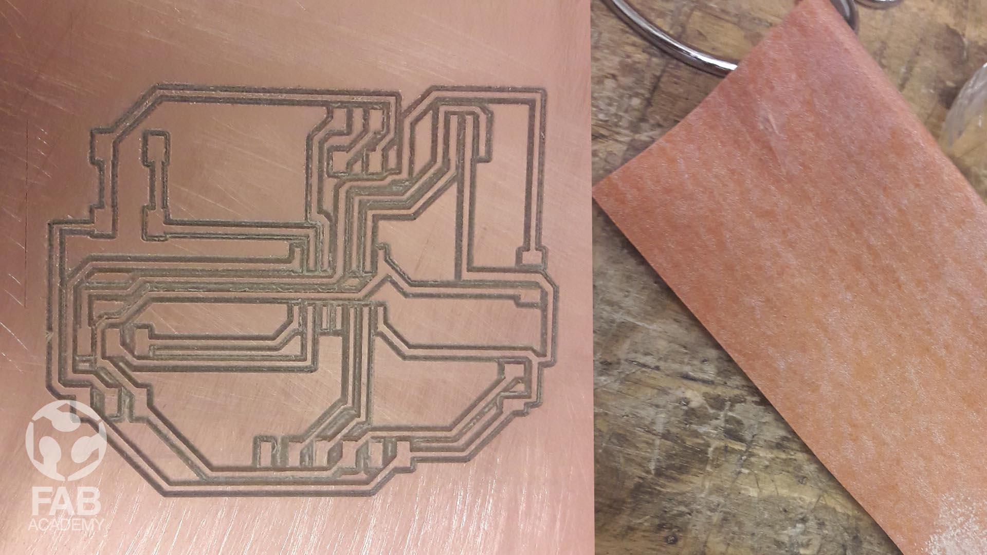
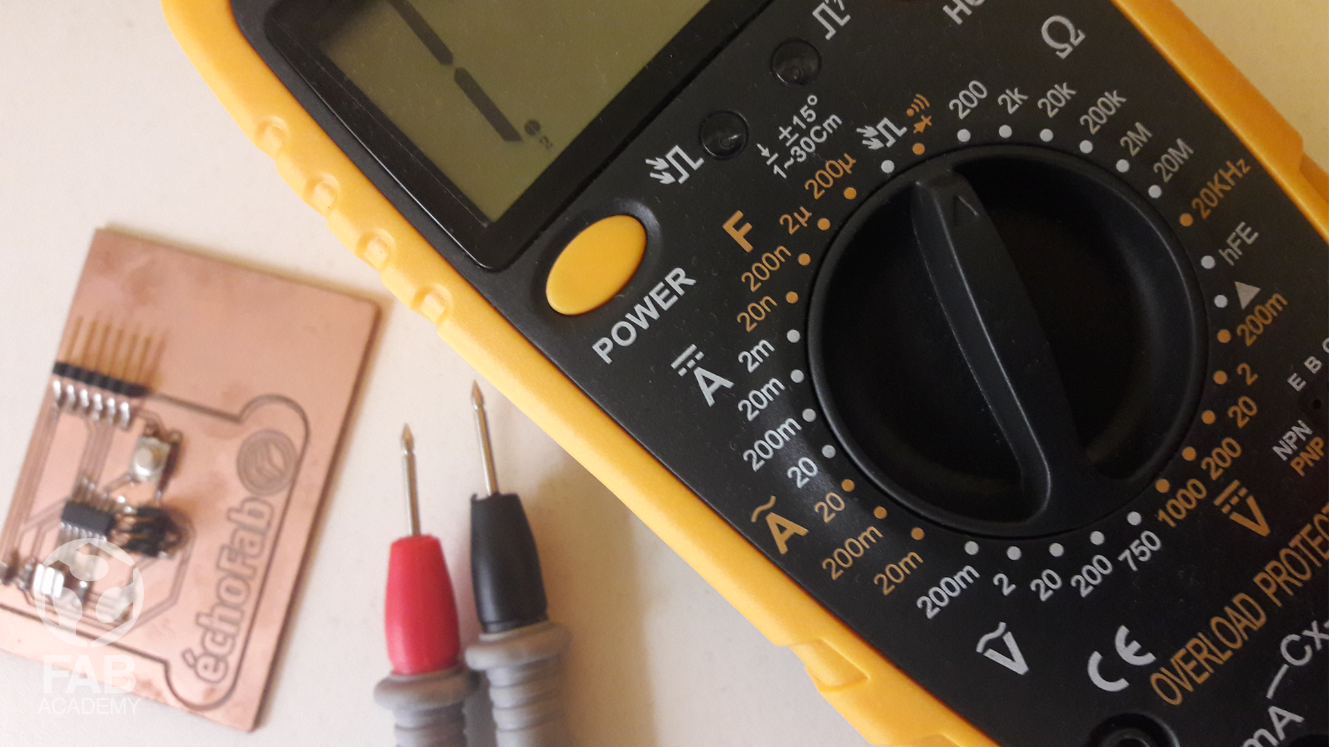
After finalizing milling the PCB I used the multimeter to test the traces to check if there is a any short
However, to do that first I inserted the black lead into the COM jack and then I interested the red lead into the V Ω jack and I turned on the multimeter
and then I adjusted the multimeter knob to the continuity function as shown in image # 21 and I placed the two test leads on two different points on close traces to make sure that the traces are not touching
each other as show in image # 22
USEFUL TIPS & LINKS
+ The download link for EAGLE software HERE.
+ The download link for Hello Echo example HERE.
+ The download link for FAB Library HERE.
DOWNLOAD SECTION
+ HELLO WORLD_TRACES.png DOWNLOAD .
+ HELLO WORLD_OUTLINE.png DOWNLOAD .
+ helloboard.brd DOWNLOAD .
+ helloboard.sch DOWNLOAD .